


Rigaku Corporation, a global solution partner in X-ray analytical technology and a group company of Rigaku Holdings Corporation (Headquarters: Akishima, Tokyo; CEO: Jun Kawakami; hereinafter “Rigaku”), has received two awards at the 2026 Local Commendation for Invention, organized by the Japan Institute of Invention and Innovation.
The company received the Osaka Governor’s Award (Special Award) and the Invention Encouragement Award for two patented technologies related to semiconductor X-ray analysis and metrology. This marks Rigaku’s fourth consecutive year of receiving a Special Award.
Building on this recognition, Rigaku will continue to develop technologies that address analytical and metrology challenges in the semiconductor industry and beyond.
Special Award
X-ray Fluorescence Analysis Enabling High-Precision Characterization of Advanced Semiconductor Substrates
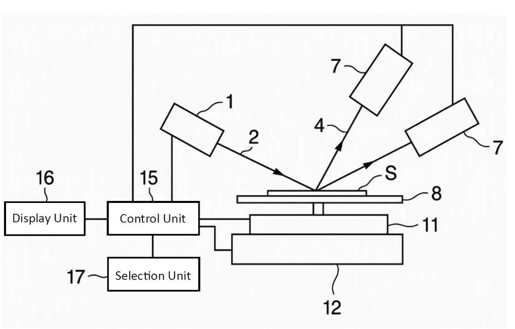
This invention uses X-ray fluorescence (XRF) technology to accurately analyze advanced semiconductor substrates, such as gallium nitride (GaN). In conventional methods, X-rays diffracted by the crystal structure can interfere with the fluorescent X-rays used for analysis, making accurate measurements difficult.
Conventional methods for silicon substrates use two measurement angles, 180 degrees apart, to avoid this interference. This invention instead measures diffracted X-rays while rotating the substrate through 360 degrees, allowing three or more suitable measurement angles to be selected. By reducing interference while minimizing the need to move the substrate, the technology enables highly accurate measurement of the thickness and elemental composition of thin films. It contributes to quality control in advanced semiconductor manufacturing.
Award Name: Kinki Local Commendation for Invention “Osaka Governor’s Award”
Invention Name: X-ray Fluorescence Analytical Apparatus and Method (Patent No. 4914514)
Inventor: Hiroshi Kobayashi
Product Details: WDA3650, WaferX 310
Invention Encouragement Award
In-Line X-ray Metrology Enabling High-Precision Characterization of Microscopic Areas in Semiconductor Thin Films
As semiconductor devices become more advanced, three-dimensional structures using superlattice thin films, such as Si/SiGe (silicon-germanium), are becoming more common. The properties of these thin films directly affect device performance, making precise metrology in microscopic areas essential. However, conventional X-ray techniques have struggled to achieve both high accuracy and the ability to measure such small areas.
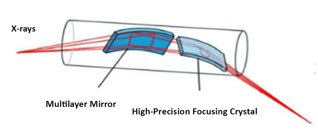
This invention uses a newly developed X-ray optical system that combines a high-precision focusing crystal with a multilayer mirror. By focusing X-rays onto areas approximately 50 micrometers in size while maintaining high angular resolution, the system enables fast and accurate measurement of thin-film composition, crystallinity, and crystal strain during manufacturing. This contributes to more consistent product quality and improved manufacturing yields for advanced semiconductors.
Award Name: Kanto Local Commendation for Invention “Invention Encouragement Award”
Invention Name: X-ray Metrology Apparatus, X-ray Thin-Film Characterization Method, and Rocking Curve Measurement Method (Patent No. 6864888)
Inventors: Kiyoshi Ogata, Kazuhiko Omote, Sei Yoshihara, Yoshiyasu Ito, Hiroshi Motono, Hideaki Takahashi, Takao Kinebuchi, Akifusa Higuchi, Shiro Umegaki, Shigematsu Asano, Ryotaro Yamaguchi, Katsutaka Horada, Makoto Kanbe, Licai Jiang, Boris Verman
Product Details: XTRAIA XD-3300
About the Rigaku Group
Since its establishment in 1951, the engineering professionals of the Rigaku Group have been dedicated to benefiting society with leading-edge technologies, notably including its core fields of X-ray and thermal analysis. With a market presence in 136 countries and regions and more than 2,000 employees worldwide, Rigaku is a solution partner for industrial and research analytical applications. Our overseas sales ratio has reached approximately 70% while sustaining an exceptionally high market share in Japan. Together with our customers, we continue to develop and grow. As applications expand from semiconductors, electronic materials, batteries, environment, resources, energy, and life sciences to other high-tech fields, Rigaku realizes innovations “To Improve Our World by Powering New Perspectives.” For details, please visit rigaku-holdings.com/english.
Press Contact:
Sawa Himeno
Director, Communications Dept., Rigaku Holdings Corporation
prad@rigaku.co.jp